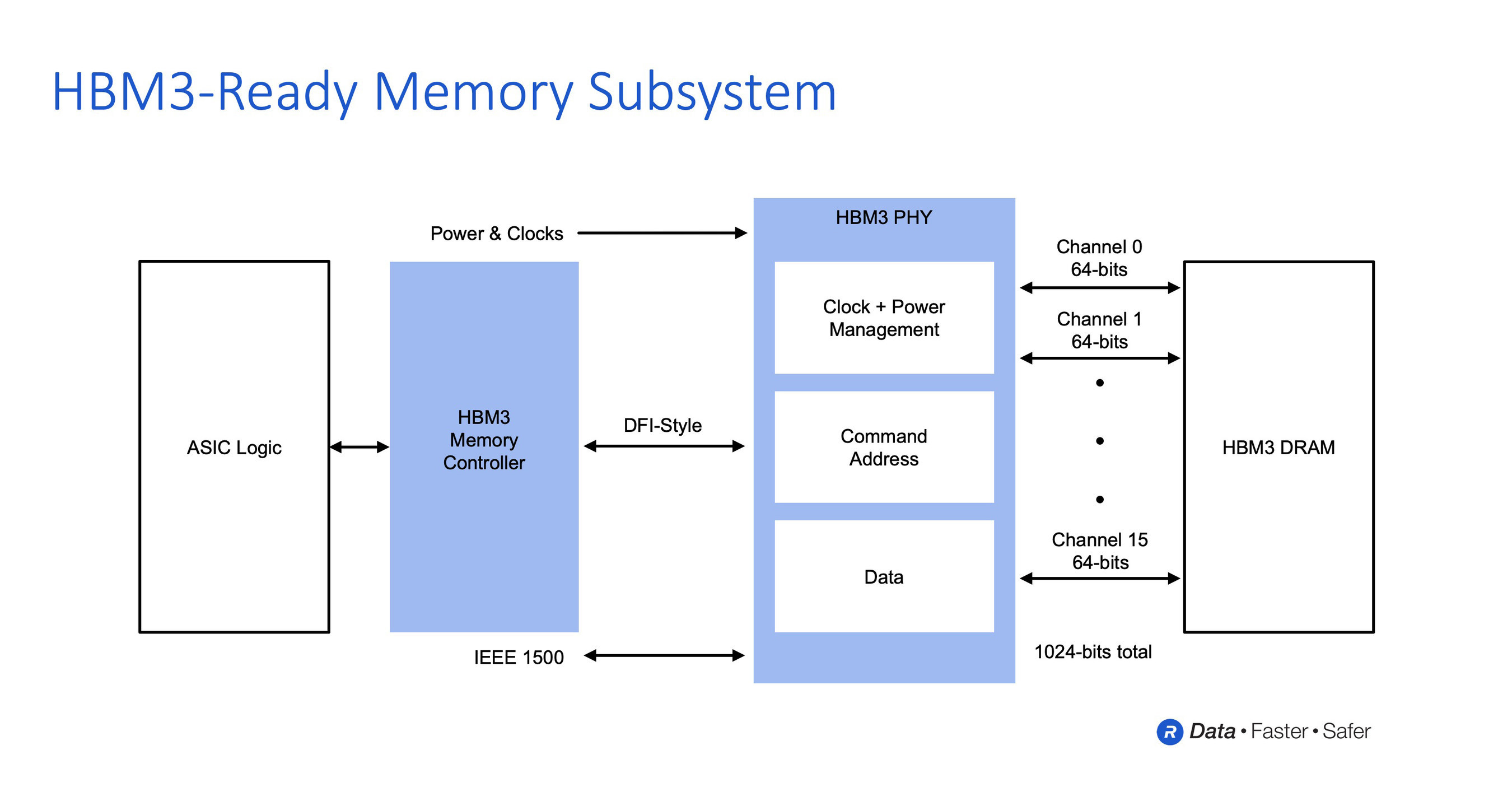
SAN JOSE, California, August 16, 2021 / PRNewswire / – Rambus inc. (NASDAQ: RMBS), a leading provider of silicon chips and IPs that make data faster and more secure, today announced the Rambus HBM3 Ready Memory Interface Subsystem, consisting of a fully integrated PHY and digital controller. Supporting breakthrough data rates of up to 8.4 Gbps, the solution can deliver over one terabyte per second of bandwidth – more than double that of high-end HBM2E memory subsystems . With a market leading position in HBM2 / 2E memory interface deployments, Rambus is ideally suited to enable customers to implement accelerators using next generation HBM3 memory.
“The memory bandwidth requirements of AI / ML training are insatiable with leading-edge training models now exceeding billions of parameters,†said Soo Kyoum Kim, Associate Vice President, Memory Semiconductors at IDC. “The Rambus HBM3 Ready Memory Subsystem raises the bar for performance enabling state-of-the-art AI / ML and HPC applications. ”
Rambus achieves HBM3 operation at up to 8.4 Gbps leveraging over 30 years of high-speed signaling expertise and a strong history of designing and activating 2.5D memory system architecture. In addition to the fully integrated memory subsystem ready for HBM3, Rambus provides its customers with reference interposer and enclosure designs to accelerate their products to market.
“With the performance achieved by our HBM3 compatible memory subsystem, designers can deliver the bandwidth needed for the most demanding designs,” said Matt jones, Managing Director of Interface IP at Rambus. “Our fully integrated PHY and digital controller solution builds on our large installed base of HBM2 customer deployments and leverages a comprehensive suite of support services to ensure proper first implementation for AI designs / ML reviews. ”
Benefits of the Rambus HBM3 Compatible Memory Interface Subsystem:
- Supports data rate up to 8.4 Gbps providing a bandwidth of 1.075 terabytes per second (TB / s)
- Reduces ASIC design complexity and speeds time to market with fully integrated PHY and digital controller
- Provides full bandwidth performance in all data traffic scenarios
- Supports HBM3 RAS features
- Includes a built-in hardware-level performance activity monitor
- Provides access to the Rambus system and SI / PI experts helping ASIC designers ensure maximum signal and power integrity for devices and systems
- Includes 2.5D package and interposer reference design as part of IP license
- Includes the LabStation â„¢ development environment that enables rapid system set-up, characterization and debugging
- Enables the best performance in applications including advanced AI / ML training and high performance computing (HPC) systems
For more information on the Rambus interface IP, including our PHYs and controllers, please visit rambus.com/interface-ip.
Follow Rambus:
Company website: rambus.com
Rambus blog: rambus.com/blog
Twitter: @rambusinc
LinkedIn: www.linkedin.com/company/rambus
Facebook: www.facebook.com/RambusInc
About Rambus inc.
Rambus is a supplier of advanced silicon chips and IPs that make data faster and more secure. With over 30 years of advanced semiconductor experience, we are a pioneer in high performance memory subsystems that solve the bottleneck between memory and processing for data intensive systems. Whether in the cloud, at the edge, or in your hand, real-time and immersive applications depend on throughput and data integrity. Rambus products and innovations deliver the increased bandwidth, capacity and security needed to meet the world’s data needs and deliver ever greater experiences for end users. For more information, visit rambus.com.
Press contact:
Cori Pasinetti
Rambus corporate communication
Phone. : (650) 309-6226
[email protected]
SOURCE Rambus Inc.
Related links
https://www.rambus.com/